
- Home
- Forums
- General Area
- Off-Topic Chat
- Art's Studies
You are using an out of date browser. It may not display this or other websites correctly.
You should upgrade or use an alternative browser.
You should upgrade or use an alternative browser.
Welcome to our Community
Wanting to join the rest of our members? Feel free to sign up today.
Sign up
Well, i've decided to give it a try, cos i'm a bit desperate here...
Guys, who is familiar with VHDL and ALTERA development kit?
ask me if you arrived the point "porn" :thanks:
Well, i've decided to give it a try, cos i'm a bit desperate here...
Guys, who is familiar with VHDL and ALTERA development kit?
ask me if you arrived the point "porn" :thanks:
i'm there right now
 in the arse
Whats that Arthur? lol
eehm, it's a programming tool that describes electronic hardware - sometimes it's a complete "porn" when you don't know what to do... and how to proceed
lool
what are u studying then exactly
Electrical engineering, BSc - and yes Steffos, it's a part of my studies too. In addition I have digital hardware design. My question is related to that issue.
sounds better than the chemistry shite I did ..... you only have one chance at this and at times it will seem like complete bollocks but try to do it with the best effort you can. it may be the making of you in the future ...... or just quit it now and do something you enjoy ....maybe a fish farmer ? lol Isreali Koi ?what are u studying then exactly
Electrical engineering, BSc - and yes Steffos, it's a part of my studies too. In addition I have digital hardware design. My question is related to that issue.
i can't quit - i will graduate this semester
lol and i have some chemistry too, about semiconductors lool
I did VHDL years ago m8 in a previous company, company I'm in atm it's all verilog. We use both Xilinx and Altera for FPGA prototyping. The toolchains are very similar.
What you trying to do ? Maybe I can help a bit
yawnnn...Boring bit -> (I have a B.Eng(Hons) in Electronic Enginering and a BTEC HND in Electrical & Electronic engineering, currently an Applications Enginner with Analog devices supporting video ICs mostly focused on automotive, here is a part we recently released that accepts 2xHDMI inputs, I2C,GPIOs, SPI, MII(for ethernet) and sends them all over a high speed serial link(3Gbps) ADV7682 datasheet and product info | APIX2 Transmitter with Dual Port HDMI and HDCP Support | Analog/HDMI/DVI Interfaces | Analog Devices)
You COCK! I've spent a fortune to buy ICs from analog devices! My whole project is based on them.
My project deals with CCD sensor - it will be a video camera (or should be) lol Anyways, lets stay in focus. I have a design that working perfectly when simulating it in ModelSim, then when i program the FPGA (Cyclon 4E) - i have output ports that provide me with correct signal, and several outputs that are not functioning.
Meaning, no signal at all, incorrect frequency, or just '1'.
When checking back warnings, pinout, RTL - nothing suspicious (to me) .
The complete design should control CCD sensor in a matter of timing and extracting data from it.
My project deals with CCD sensor - it will be a video camera (or should be) lol
Anyways, lets stay in focus. I have a design that working perfectly when simulating it in ModelSim, then when i program the FPGA (Cyclon 4E) - i have output ports that provide me with correct signal, and several outputs that are not functioning. Meaning, no signal at all, incorrect frequency, or just '1'.
When checking back warnings, pinout, RTL - nothing suspicious (to me) .
The complete design should control CCD sensor in a matter of timing and extracting data from it.
I use QUARTUS as a development environment. The design is based on state machine that enables procedures in order to enforce specific situation of outputs. It all works fine - but on TEST BENCH only
I know about VERILOG - but, only theoretically a bit. Never used it yet.
Thank you for your interest Mini, and your help
Say "HI!" from me to Analog Devices.
Let's see your datasheet there....
I know about VERILOG - but, only theoretically a bit. Never used it yet.
Thank you for your interest Mini, and your help
Say "HI!" from me to Analog Devices.
Let's see your datasheet there....
Ok lets go.
Firstly if I start to say stuff that you know well about and you think 'jesus this guy, I'm not an idiot' then my apologises upfront
Working on testbench is brilliant ! That at least shows your behavioural model is ok. When it comes to the gatelevel in the FPGA we have to remeber timing is going to come into play.
Few things to get us warmed up.
Make sure that ALL your used outputs and inputs in the design go to a FPGA pin. At synthesis if an logic output dosent go to a pin then the synthesis tool will consider that logic redundant and optimise it away ! Like wise an unconnected Input will get connected to either '1' or '0' internally by the synthesis.
Check the synthesis report for logic being optimised away. Also check the synthesis tool to see that its infering the logic that you expected. You said your design was statemachine based make sure that the synthesis tool is picking up that you have a state machine, it should tell you in the report that is sees a statemachine with x ammount of states. Confirm that you do indeed have that many states in your design. Also check to make sure the tool isnt flagging that you have unreachable states.
Clocks & Reset.
Maybe some basics here, again sorry if I'm preaching. In a testbench its easy to generate a clock. Where in you design is the clock ? Is it internally generated or fed in from outside ? On clocking its better to always only stick to using only one clock edge (pos or neg, dosent matter) In testbench you will be fine cause you have made a nice 50% duty cycle clock but in real life a xtal oscillator clock maybe as bad as 80/20 duty cycle. This will give you more headaches than its worth if you are trying clock stuff on different clock edges.
TDR Pick a clock edge and stick to it
I hope to god you are using a GLOBAL reset to get all your logic into a nice state ? Also for the love of God please use a synchronous reset in your design.
In test bench resets are easy peasy....How are you generating a reset for your FPGA ? A good way is to use a external push button switch connected to a FPGA IO. This signal will not be synchronous to your system clock as you could press it at any time, as this signal comes into your FPGA, actually let me start that again.
Any signal that comes into your FPGA that is NOT based off the system clock is asynchronous and needs to be made synchronus in order to avoid metastability.
Easiset thing to do is to pass the Async signal through 2 D-type flipflops.
Simulation Models.
I assume its behavioural level that you did in modelsim. In the quartus tools it should generate for you other simulation models
after synthesis
after place/fit/route in the FPGA
These would be worth simulating to see if your design has any timing issues. The end result simulation model will have the timing due to the internal routing within the FPGA and any logic delays.
This should be as close to what you see on the bench in real life.
Timing Constraints.
Do you have any timing constraints set ? At the most basic level you need to at least let the tools know your system clock speed. The tools needs this info when doing place and route in order to make sure all the logic meets setup and hold timing internally. Check for a timing report and see if you have any setup/hold violations. the timing report should also give a maximum speed your design can be clocked at. if the timing report says max 25Mhz and you know that you are using a 80Mhz clock then you know you are gonna have issues. Conversly if he reports max 80Mhz and your actual clock is only 25Mhz then you can be pretty confident that you will be ok.
Timing violations and issues can be tricky to resolve but usually pipelineing is alls thats needed. Pipelineing is adding flip-flop stages to a signal in order to break up a long timing path, it addes a clock delay to your signal but you can work with that.
Without seeing any code, reports, block diagrams etc its hard to know what to point at art.
But to start with....Clocks, resets, synthesis reports !
A handy debug idea is to bring out your current state signals (say currentstate[4:0] then bring those 5 signals out to IOs and scope them.... Apply reset to your logic and see if the current state goes through the states you expect ! if it stays static then is your statemachine getting the right inputs in order to make it progress to the next state ? !
On statemachines always have a state that you goto after a system reset ! It makes debugging Statemachines much easier !
I've thrown a bit out here and I'm sorry if its too much or even if its all old news to you.
let me know how you are getting on with the above and maybe it rings some bells as to where to look further. Feel free to ask any questions or if you want me to go into more detail on anything.
Firstly if I start to say stuff that you know well about and you think 'jesus this guy, I'm not an idiot' then my apologises upfront
Working on testbench is brilliant ! That at least shows your behavioural model is ok. When it comes to the gatelevel in the FPGA we have to remeber timing is going to come into play.
Few things to get us warmed up.
Make sure that ALL your used outputs and inputs in the design go to a FPGA pin. At synthesis if an logic output dosent go to a pin then the synthesis tool will consider that logic redundant and optimise it away ! Like wise an unconnected Input will get connected to either '1' or '0' internally by the synthesis.
Check the synthesis report for logic being optimised away. Also check the synthesis tool to see that its infering the logic that you expected. You said your design was statemachine based make sure that the synthesis tool is picking up that you have a state machine, it should tell you in the report that is sees a statemachine with x ammount of states. Confirm that you do indeed have that many states in your design. Also check to make sure the tool isnt flagging that you have unreachable states.
Clocks & Reset.
Maybe some basics here, again sorry if I'm preaching. In a testbench its easy to generate a clock. Where in you design is the clock ? Is it internally generated or fed in from outside ? On clocking its better to always only stick to using only one clock edge (pos or neg, dosent matter) In testbench you will be fine cause you have made a nice 50% duty cycle clock but in real life a xtal oscillator clock maybe as bad as 80/20 duty cycle. This will give you more headaches than its worth if you are trying clock stuff on different clock edges.
TD
R Pick a clock edge and stick to it I hope to god you are using a GLOBAL reset to get all your logic into a nice state ? Also for the love of God please use a synchronous reset in your design.
In test bench resets are easy peasy....How are you generating a reset for your FPGA ? A good way is to use a external push button switch connected to a FPGA IO. This signal will not be synchronous to your system clock as you could press it at any time, as this signal comes into your FPGA, actually let me start that again.
Any signal that comes into your FPGA that is NOT based off the system clock is asynchronous and needs to be made synchronus in order to avoid metastability.
Easiset thing to do is to pass the Async signal through 2 D-type flipflops.
Simulation Models.
I assume its behavioural level that you did in modelsim. In the quartus tools it should generate for you other simulation models
after synthesis
after place/fit/route in the FPGA
These would be worth simulating to see if your design has any timing issues. The end result simulation model will have the timing due to the internal routing within the FPGA and any logic delays.
This should be as close to what you see on the bench in real life.
Timing Constraints.
Do you have any timing constraints set ? At the most basic level you need to at least let the tools know your system clock speed. The tools needs this info when doing place and route in order to make sure all the logic meets setup and hold timing internally. Check for a timing report and see if you have any setup/hold violations. the timing report should also give a maximum speed your design can be clocked at. if the timing report says max 25Mhz and you know that you are using a 80Mhz clock then you know you are gonna have issues. Conversly if he reports max 80Mhz and your actual clock is only 25Mhz then you can be pretty confident that you will be ok.
Timing violations and issues can be tricky to resolve but usually pipelineing is alls thats needed. Pipelineing is adding flip-flop stages to a signal in order to break up a long timing path, it addes a clock delay to your signal but you can work with that.
Without seeing any code, reports, block diagrams etc its hard to know what to point at art.
But to start with....Clocks, resets, synthesis reports !
A handy debug idea is to bring out your current state signals (say currentstate[4:0] then bring those 5 signals out to IOs and scope them.... Apply reset to your logic and see if the current state goes through the states you expect ! if it stays static then is your statemachine getting the right inputs in order to make it progress to the next state ? !
On statemachines always have a state that you goto after a system reset ! It makes debugging Statemachines much easier !
I've thrown a bit out here and I'm sorry if its too much or even if its all old news to you.
let me know how you are getting on with the above and maybe it rings some bells as to where to look further. Feel free to ask any questions or if you want me to go into more detail on anything.
Thank you a lot, Mini, for your help. I'm already familiar with problems that you've described for me. I used the same approach to troubleshoot things with TestBench. I think post synthesis summary might be useful for me - what should i check there? (in relation to my problem)
I was browsing through these reports recently, but I didn't find anything specific. It's A LOT of long long text files there.
Where should I concentrate more attention? In regarding to those reports. This is my major question to you now
My clock is GLOBALLY distributed, so is my RESET. Hold/Setup problems shouldn't rise at all, IMO, because i'm using less than 1% of device resources.
In addition, in my case, i have a signal that has to be about 10MHz, but i have it on 2KHz instead, with same DutyCycle. The 2KHz frequency is planned for other signal, on other pin, but it never appeared.
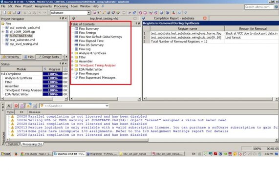
All my ports (in/out) are registered in pin planner. I just can't find signals that where "optimized away" lol and i don't know how to do it, cos i didn't find any warning about it.
I think post synthesis summary might be useful for me - what should i check there? (in relation to my problem)I was browsing through these reports recently, but I didn't find anything specific. It's A LOT of long long text files there.
Where should I concentrate more attention? In regarding to those reports. This is my major question to you now
My clock is GLOBALLY distributed, so is my RESET. Hold/Setup problems shouldn't rise at all, IMO, because i'm using less than 1% of device resources.
In addition, in my case, i have a signal that has to be about 10MHz, but i have it on 2KHz instead, with same DutyCycle. The 2KHz frequency is planned for other signal, on other pin, but it never appeared.
All my ports (in/out) are registered in pin planner. I just can't find signals that where "optimized away"
lol and i don't know how to do it, cos i didn't find any warning about it.Attachments
Synthesis reports are kinda big but they should be broke down by block or module level in VHDL it would be architrectures or entityies...
What you are looking for is that the synthesis tool had created the logic rougly that you expected.
For example if I knew I had a 16 bit counter and some registers in a section of my design and when I look at my synthesis report its saying for that section it found a d-type flip flop then I know that something is amiss...either the inputs to that block are not used or the outputs form that block are not used anywhere else in the design hence the synthesis tool will just optimise the logic away as its redundant.
In your screenshot we can already see that synthesis has removed 12 registers.... Now sometimes thats ok. Remember that the synthesis is taking your design and more or less doing a logic reduction on it...Its very good at this and on paper it would take you hours if not days
Its more or less doign the same thing you did back in first year digitial design of comming up with a truth table and reducing it down to the miminal logic needed using Karnaugh maps, DeMorgans laws etc.
So long story short, sometimes its goign to remove registers or logic that is not needed but you really need to have an idea of the logic that the synthesis SHOULD infer.
On this point 'My clock is GLOBALLY distributed, so is my RESET. Hold/Setup problems shouldn't rise at all, IMO, because i'm using less than 1% of device resources.'
Normally I'd agree with you, if a FPGA is only using about 1% of resources then you'd expect that it should have no trouble to meet timing but it all depends if your timing paths are long due to logic delay or routing delay.
In a unutilised FPGA you'd expect the routing delay to be quite small as during place and route there is so many options for the Placer to work with. Your design may be fundamentally LOGIC bound and its just the massive lump of logic that you have that is causing timing issues. In this case normally you just break up the logic into pipelined stages.... i.e add registers
Saying that it is good practice to register Inputs and outputs both to/from the FPGA and also between the internal blocks/modules/entiteies. Are you doing this ?
Also there is options for the Placer to push the IO registers into the IOBs (this is how it works for Xilinx, i'll have to check that altera is similar)
Did you try simulating the post synthesis simulaton model and see if that works similar to the behavioral level ? If its all good here then the issue is more than likely due to the next stages -> MAP, PLACE/ROUTE or timing.
How did you see that 12 registers wiped away from my design??? I'm aware of that, that all the 1st year paper work is done behind the scenes of QUARTUS, thank GOD it's so! But... How do you see it already from my screenshot?
MiNi you just read my mind. That's exactly what i'm doing right now, breaking the whole program into small components, with same clock/reset, and wiring them together, when adding smpling FFs for input signal and for output signals.
The post synthesis simulation, i would like to do, but i don't know how - yet.
Is it somewhere over here, on screenshot?
But... How do you see it already from my screenshot? MiNi you just read my mind. That's exactly what i'm doing right now, breaking the whole program into small components, with same clock/reset, and wiring them together, when adding smpling FFs for input signal and for output signals.
The post synthesis simulation, i would like to do, but i don't know how - yet.
Is it somewhere over here, on screenshot?
Attachments
Very first screen shot look you posted far right
In Xilinx to generate the post synthesis sim model Generating a Post-Synthesis Simulation Model
On Altera I'm not so sure (we have Altera & Xilinx but all of my FPGA work recently has been Xilinx) Poke around in the tools and in the folders you should find the synthesised netlist.
When it comes to sim you usually have to include the Altera libraries when invoking vsim. In xilinx when using the ISE tools it will pass the correct vsim command to modelsim depending on which sim model you want to run

Bit of a Altera related thread here might help you out -> post-synthesis simulation of a quartus design in modelsim
Sorry I'm not more help on Altera, atm I'm more Xilinx focused....On Monday when I'm back at work I can talk to some of the designers using Altera toolchain and pump them for info
In Xilinx to generate the post synthesis sim model Generating a Post-Synthesis Simulation Model
On Altera I'm not so sure (we have Altera & Xilinx but all of my FPGA work recently has been Xilinx) Poke around in the tools and in the folders you should find the synthesised netlist.
When it comes to sim you usually have to include the Altera libraries when invoking vsim. In xilinx when using the ISE tools it will pass the correct vsim command to modelsim depending on which sim model you want to run
Bit of a Altera related thread here might help you out -> post-synthesis simulation of a quartus design in modelsim
Sorry I'm not more help on Altera, atm I'm more Xilinx focused....On Monday when I'm back at work I can talk to some of the designers using Altera toolchain and pump them for info

Users who are viewing this thread
Total: 1 (members: 0, guests: 1)
- Home
- Forums
- General Area
- Off-Topic Chat
- Art's Studies